相關主題

商品描述
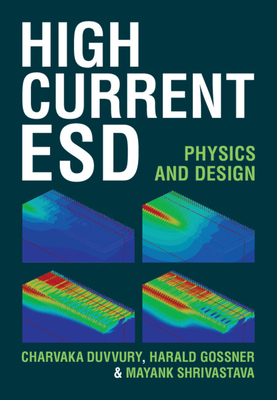
Covering a wide spectrum of semiconductor technologies, this book offers comprehensive description of the physics of electrostatic discharge (ESD) phenomena that incorporate and lead to robust on-chip protection design practices. Starting with fundamental insights into high-current ESD behavior in semiconductor devices, it gradually builds toward practical design principles and real-world reliability challenges in advanced complementary metal oxide semiconductor (CMOS), fin field-effect transistor (FinFETs), gallium nitride high-electron-mobility transistors (GaN HEMTs), carbon nanostructures, and thin film transistor (TFT) technologies. Device-level physics and practical design implications are explored throughout, bridging the gap between deep theoretical understanding and real-world design constraints. Including unique simulation techniques alongside experimental results, this book thoroughly explores core ESD design principles. With multiple curated case studies, this book will equip readers with the tools to address current ESD design challenges and prepare for future ones. A reliable and thought-provoking exploration, this book will be ideal for graduate students, industry professionals, and researchers working in device physics, design, and reliability.
商品描述(中文翻譯)
本書涵蓋了廣泛的半導體技術,提供了對靜電放電(Electrostatic Discharge, ESD)現象的全面描述,這些現象融入並促進了穩健的晶片內保護設計實踐。從對半導體器件中高電流ESD行為的基本見解開始,逐步建立實用的設計原則和先進互補金屬氧化物半導體(Complementary Metal Oxide Semiconductor, CMOS)、鳍式場效應晶體管(FinFETs)、氮化鎵高電子遷移率晶體管(Gallium Nitride High-Electron-Mobility Transistors, GaN HEMTs)、碳納米結構和薄膜晶體管(Thin Film Transistor, TFT)技術中的現實可靠性挑戰。全書探討了器件層面的物理學和實際設計的影響,彌合了深刻的理論理解與現實設計限制之間的差距。書中包括獨特的模擬技術和實驗結果,徹底探討了核心的ESD設計原則。透過多個精心策劃的案例研究,本書將為讀者提供應對當前ESD設計挑戰的工具,並為未來的挑戰做好準備。這本可靠且引人深思的探索將非常適合研究生、行業專業人士以及從事器件物理、設計和可靠性的研究人員。


